- 您现在的位置:买卖IC网 > Sheet目录2010 > MAX5307EUE+ (Maxim Integrated Products)IC DAC 12BIT OCT LP SER 16-TSSOP
MAX5306/MAX5307
Power-Supply Considerations
On power-up, all input and DAC registers are cleared
and DOUT is in low.
Bypass VDD to GND with a 4.7F capacitor in parallel
with a 0.1F capacitor. Use short lead lengths and
place the bypass capacitors as close to the supply
pins as possible.
Low-Power, Low-Glitch, Octal 12-Bit Voltage-
Output DACs with Serial Interface
12
______________________________________________________________________________________
SCLK
X
1
2
3
4
16
D1
D12
D14
X
DIN
X
DOUT
D14*
D13*
D12*
D1*
CS
tCSH
tCL
tDH
tDS
tCSS
tCH
tSDL
tSDH
tCSPWH
D0
D0*
D15*
D15
D13
*PREVIOUS INPUT DATA
±0.5LSB
VOUT_
tCLRPWL
tLDACPWL
tS
CLR
LDAC
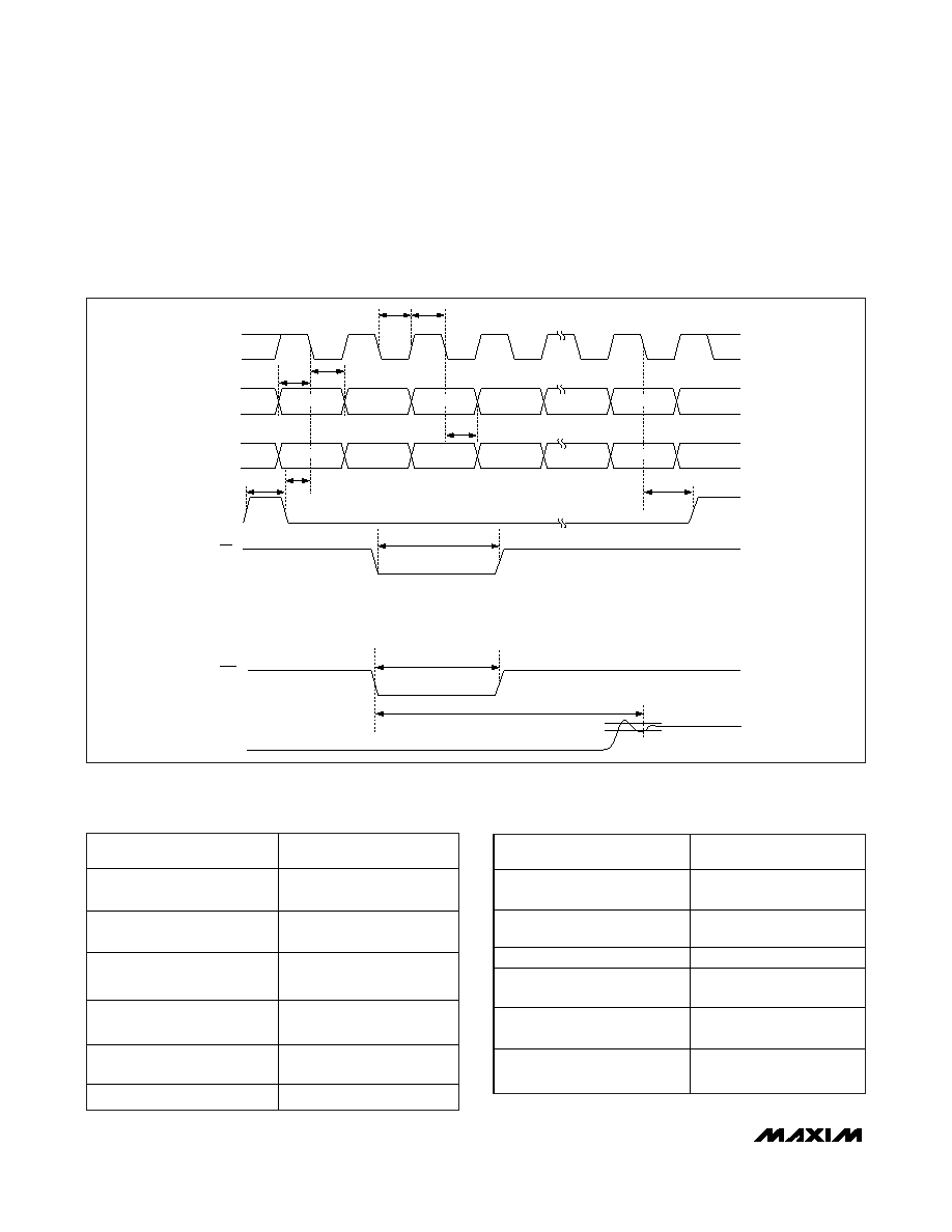
Figure 4. Timing Diagram
DAC CONTENTS
ANALOG OUTPUT
MSB
LSB
2047
1111
+VREF ( ——— )
2048
1
1000
0000
0001
+VREF ( ——— )
2048
1000
0000
0V
1
0111
1111
-VREF ( ——— )
2048
2047
0000
0001
-VREF ( ——— )
2048
0000
-VREF ( ——— ) = -VREF
2048
DAC CONTENTS
ANALOG OUTPUT
MSB
LSB
4095
1111
+VREF ( ——— )
4096
2049
1000
0000
0001
+VREF ( ——— )
4096
2048
+VREF
1000
0000
+VREF ( ——— ) = ————
4096
2
2047
0111
1111
+VREF ( ——— )
4096
1
0000
0001
+VREF ( ——— )
4096
0000
0V
Table 3. Unipolar Code Table
Table 4. Bipolar Code Table
发布紧急采购,3分钟左右您将得到回复。
相关PDF资料
MAX5312EAE+T
IC DAC 12BIT 5V/10V SER 16-SSOP
MAX5316GTG+
IC DAC 16BIT SPI 24TQFN
MAX5322EAI+
IC DAC 12BIT DUAL 10V SER 28SSOP
MAX532AEPE+
IC MDAC 12BIT DUAL SER 16-DIP
MAX5355EUA+
IC DAC 10BIT 3.3V VOLT OUT 8UMAX
MAX5362PEUK+T
IC DAC 6BIT LP 2WIRE SER SOT23-5
MAX5365EUT+T
IC DAC 6BIT LP 3WIRE SER SOT23-6
MAX536BEWE+
IC DAC 12BIT QUAD CALIB 16-SOIC
相关代理商/技术参数
MAX5307EUE+T
功能描述:数模转换器- DAC 12-Bit 8Ch Precision DAC RoHS:否 制造商:Texas Instruments 转换器数量:1 DAC 输出端数量:1 转换速率:2 MSPs 分辨率:16 bit 接口类型:QSPI, SPI, Serial (3-Wire, Microwire) 稳定时间:1 us 最大工作温度:+ 85 C 安装风格:SMD/SMT 封装 / 箱体:SOIC-14 封装:Tube
MAX5307EUE-T
功能描述:数模转换器- DAC RoHS:否 制造商:Texas Instruments 转换器数量:1 DAC 输出端数量:1 转换速率:2 MSPs 分辨率:16 bit 接口类型:QSPI, SPI, Serial (3-Wire, Microwire) 稳定时间:1 us 最大工作温度:+ 85 C 安装风格:SMD/SMT 封装 / 箱体:SOIC-14 封装:Tube
MAX5307EUE-TG077
制造商:Rochester Electronics LLC 功能描述: 制造商:Maxim Integrated Products 功能描述:
MAX5308EUE
功能描述:数模转换器- DAC RoHS:否 制造商:Texas Instruments 转换器数量:1 DAC 输出端数量:1 转换速率:2 MSPs 分辨率:16 bit 接口类型:QSPI, SPI, Serial (3-Wire, Microwire) 稳定时间:1 us 最大工作温度:+ 85 C 安装风格:SMD/SMT 封装 / 箱体:SOIC-14 封装:Tube
MAX5308EUE+
功能描述:数模转换器- DAC 10-Bit 8Ch Precision DAC RoHS:否 制造商:Texas Instruments 转换器数量:1 DAC 输出端数量:1 转换速率:2 MSPs 分辨率:16 bit 接口类型:QSPI, SPI, Serial (3-Wire, Microwire) 稳定时间:1 us 最大工作温度:+ 85 C 安装风格:SMD/SMT 封装 / 箱体:SOIC-14 封装:Tube
MAX5308EUE+T
功能描述:数模转换器- DAC 10-Bit 8Ch Precision DAC RoHS:否 制造商:Texas Instruments 转换器数量:1 DAC 输出端数量:1 转换速率:2 MSPs 分辨率:16 bit 接口类型:QSPI, SPI, Serial (3-Wire, Microwire) 稳定时间:1 us 最大工作温度:+ 85 C 安装风格:SMD/SMT 封装 / 箱体:SOIC-14 封装:Tube
MAX5308EUE-T
功能描述:数模转换器- DAC RoHS:否 制造商:Texas Instruments 转换器数量:1 DAC 输出端数量:1 转换速率:2 MSPs 分辨率:16 bit 接口类型:QSPI, SPI, Serial (3-Wire, Microwire) 稳定时间:1 us 最大工作温度:+ 85 C 安装风格:SMD/SMT 封装 / 箱体:SOIC-14 封装:Tube
MAX5309EUE
功能描述:数模转换器- DAC RoHS:否 制造商:Texas Instruments 转换器数量:1 DAC 输出端数量:1 转换速率:2 MSPs 分辨率:16 bit 接口类型:QSPI, SPI, Serial (3-Wire, Microwire) 稳定时间:1 us 最大工作温度:+ 85 C 安装风格:SMD/SMT 封装 / 箱体:SOIC-14 封装:Tube